ROM Programmer Tools Instruction for Use
These documents are derived from MRT Firmware Laboratory.
For more information, please visit our website http://www.mrtexp.com
ROM Programmer Tools provided by MRT can read and program ROM chip on the hard disk.,it is not only limited to hard disk, all the ROM chips in line with SPI interface, including computer motherboard BIOS chip, can use MRT Programmer Tools to brush and write and can repair the bad brush of hard disk ROM, or the bad brush of motherboard BIOS and other situations. ROM Programmer Tools as one part of MRT Tool Accessories,helps users save the cost of buying a separate programmer.
ROM Programmer Tools support all Flash Chips in line with SPI Communication Interface Specification. At present commercially available most of hard disk ROM chips, motherboard BIOS chips, a variety of PCI expansion card Option ROM chips and a variety of ROM chips of electronic digital products mostly adopts the chips in line with SPI Interface Specification, so all of them can use MRT Programmer Tools to brush and write. It is easy to recognize the SPI Chip Interface,they usually have 8 pins, making it easy to recognize.
Hardware connection:
Before using ROM Programmer Tools, firstly you need to properly connect the hardware. ROM Programmer Tools need to match MRT Programmer Seat Attachment and then can use.
Programmer Seat Attachment as shown in figure:
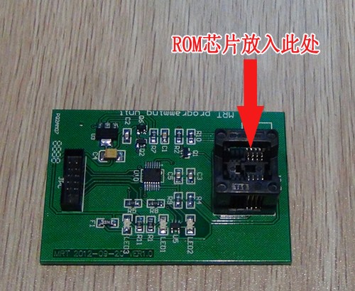
Use tweezers to place the ROM Chip needs to be programmed into the position as the arrow referred to. Attention,ROM Chip has the direction when placed,ROM Chip Notch should be consistent with the programmer seat notch as shown in above figure, or on the contrary. On the programmer seat there is power indictor (green), data read and write light and short circuit protection warning light. By observing these indicators when using, you can understand the current state of the programmer.
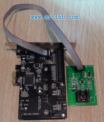
The programmer seat also needs to connect MRT hardware card and then it can be used. Connect the connecting line in the attachment to the jack of programmer seat, and connect the other end of the connecting line to the corresponding jack of MRT Hardware Card, and then insert MRT Hardware Card into PCIE Slot of the host, and then you can use it.
Attention:The use of the connecting line to connect MRT Hardware Card and the programmer seat is the little jack rather than the big jack to connect USB terminal port, please don’t mix.
The connecting between Programmer Seat and MRT Hardware Card as shown below:
Connection diagram 2:
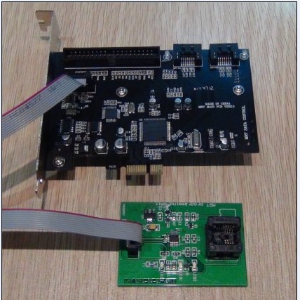
After connecting, insert MRT Hardware Card into the host PCIE slot, then you can use it.
Software Instructions:
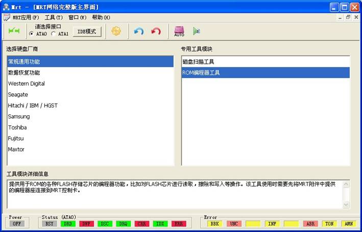
Start MRT main program,ROM Programmer Tools is below "General Common Features" classification, as shown in figure:
Click to enter; it will first enter the chip model selection dialog box:
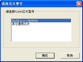
Select one model, and then click ‘OK’ to enter. If on the panel, it does not list on your chip model, you can select "other general-purpose chip" to enter.
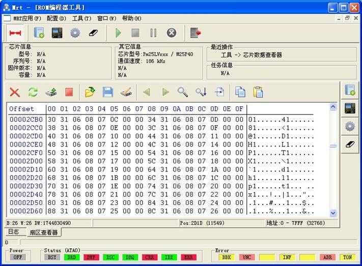
After entering, see Figure message below, it means that the programmer tool has been initialized. Below is the Programmer Tools Interface.
![USF2W]M%~5Z25IFQA]@$46A](romers.files/image006.jpg)
The interface of Programmer Tools is similar to interfaces and operation ways of other factory modules, so you can refer to the operating skills of other modules. In the upper left corner of the main toolbar there is the power switch, you can turn on or off the power on programmer seat through it. When power turns on, the power indicator on the programmer seat will light.
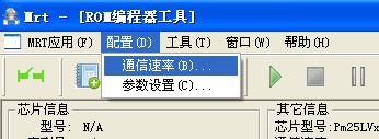
Set the communication rate:
Before beginning to use, you can firstly set the communication rate of SPT Interface. The communication rate determines the speed of reading ROM Chip. In the menu click “Configuration” -> communication rate and you can open Communication rate settings dialog.
Communication rate settings dialog as shown in figure:
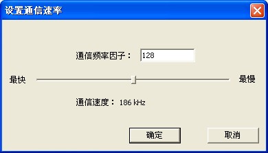
By dragging the rod, you can change the rate, the left side is the fastest, the right side is slowest, after setting the communication rate, click "OK" button to take effect.
Parameter Settings:
Click configuration on the menu -> parameter settings, can open parameter setting dialog, as shown in figure:
![Q}CFS[@4%~B57]VFJ]4HEX2](romers.files/image009.jpg)
For the setting that waits for timeout, is referred to when read and write ROM chip, if there is no response, how long to wait until exits for timeout. Usually keep the default value is 3000 milliseconds. This setting also affects the "Pause Task" function. Click “Pause Task” button on the toolbar, you can pause the currently executing task, for example the read-write of ROM Chip. When users click this button again, it can resume the task execution. Users pause longer than the task set here waiting timeout, otherwise it will exit because of the recovery task timeout. The pause task time set by users can’t exceed the waiting timeout set here; otherwise it will exit for timeout in the process of recovering task.
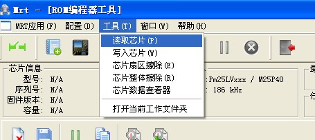
Read the chip:
Please use the "Read chip" function to read the content inside ROM chips and save it to a file. Select “Tools -> read chip”” in the main menu.
The first enter, it will appear “New Folder” dialog, as shown in below figure:
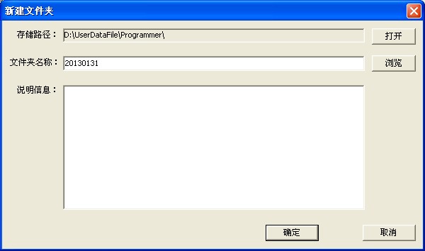
The function of dialog is consistent with other dialogs of factory module. Sometimes, we want to set up one working directory to save all the ROM chip data read and written in this period to the same file, this is the function of establishing working directory. Input the working folder name you want to set up into the "new folder" dialog box (the default date as the name), and then click OK, like this, the working folder is set up, all the backup of ROM data default later will be stored in the working folder.
Attention:If you want to open the current working folder, please select “Tools -> open the current working folder” in the main menu.
When reading the chip, after the establishment of the working folder, it will instantly pop up the chip size selection dialog box, as shown below:
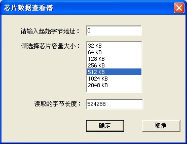
The function of this dialog is to let users to select the read range of the chip. The default is to start reading from the starting byte 0; users can also change the offset from the back of the start to read. The default chip size is 512KB, namely to read 524288 bytes. Users need to select the actual capacity of the current operation of the ROM chip. If the size of the reading exceeds the actual capacity of the chip, the programming tools will read cycle, the excess part of reading the chip is the data of the chip foremost address. If users do not clearly know the actual capacity of the current chip, users can choose the different capacities to read several times, if users find from where that the data starts cycle, then the prior of the size is the actual capacity of of the chip.
After determine the size of the chip, it will pop up the "Save As" dialog box, the default is saved in the current working directory. Users type a file name and then click “OK”, it will begin to read ROM chip, the read data will eventually be saved to the users’ specified file.
Write Into Chip:
To brush write ROM chip, please select the main menu "Tools -> write chip." After user select one file, users can write into ROM chip. User -selected data in the file will be unchangeably written into the ROM chip, the starting address of writing is the zero byte offset of ROM chip, and the write size is the user -selected file size. Attention: Write operation will firstly erase the entire chip, regardless of how great the file is written, the original data of ROM chip will be lost.
Chip Sector Erase:
If you want to erase the portion of data specified by the chip rather than erase the entire chip, you can use the sector erase function, it will only erase data of the specified sector. Select “Tools -> Chip Sector Erase” in the main menu to open it, as shown in figure below:
4H$0R3{Y$7X2K5](romers.files/image013.jpg)
Users need to fill in the starting sector number to be erased and the number of sectors to be erased in a row. Notice that the unit here is the sector instead of the byte. The sector size and sector erase instruction specified by different chips are not the same, so here "the number of bytes per sector" and "sector erase instruction code" also requires users to fill in,but we have prepared the default value, select a model in the model, it will fill in the corresponding sector byte number and the default value of instruction code. But if it is not listed the model in the dialog, it requires users to refer to the manual of chip to fill in, or try to use the default value. Attention, here's the starting sector number × number of bytes per sector = starting byte offset, the number of sectors to be erased × bytes per sector = number of bytes to be erased. This formula can calculate the sector address to be erased.
Whole Chip Erase:
Used to erase all chip data, all the chip data after erasing is changed into FF, and the new data can be written in. Generally speaking, the Write Operation can only change data bit 1into 0, but the Erase Operation is on the contrary. Therefore, firstly erase all the places where new data is to be written for FF (all 1 in binary bits) if you want to write new data. If users don't execute the erase operation before writing then according to the situation of the original data bits, newly written data may be absent,because the Write Operation can only change 1 to 0, if the bit is 0,users can't change it into 1, users need the help of the Erase Operation to achieve it. If users need to write part of data, and not willing to destroy other area’s data, users need the help of “Sector Erase” and “Chip Data Viewer”to achieve. “Chip Data Viewer”provides the option of direct writing instead of erasing.
Chip Data Viewer:
In the menu select “Tools -> Chip Data Viewer”, you can open it. The tool will read chip data and directly display it on the sixteen hex editor rather than save it to the file. Users can view and edit data in the sixteen hex editor, after the completion of editing, the chip can be directly written into.
Below is the figure of Chip Data Viewer:
When opening the tools, users need to fill in the starting address of reading, in the process of writing, it will be written into the starting address previously entered by users. When writing into, users can choose to erase before writing or not to erase the chip, if users choose not to erase, chip raw data will be retained, and mixed together with the newly written data. Users can select "Save to File" button on the toolbar to save the current data in the sixteen hex editor to a file, users can also load data into the sixteen hex editor from a file, and then re-write into the chip.
Other Descriptions:
Users can replace the ROM chips halfway, before replacing the chip programmer seat power should be turned off; you can turn on power again after the completion of replacement. In the halfway replacement, ROM chip does not need to exit the program; it takes effect immediately after the completion of replacement.
In the process of ROM chip write or erase operation, please be sure not to turn off the power halfway, otherwise it may cause damage to the chip. And in the process of write or erase operation, programmer seat must properly connect ROM chip, if the connection is not correct or not connected to ROM chip, this may result in damage to the ROM chip or MRT hardware card in the process of brushing to write.